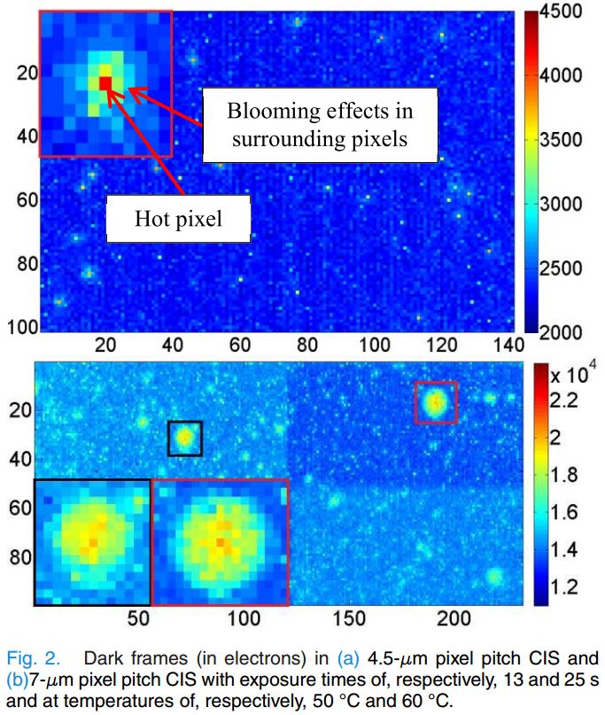
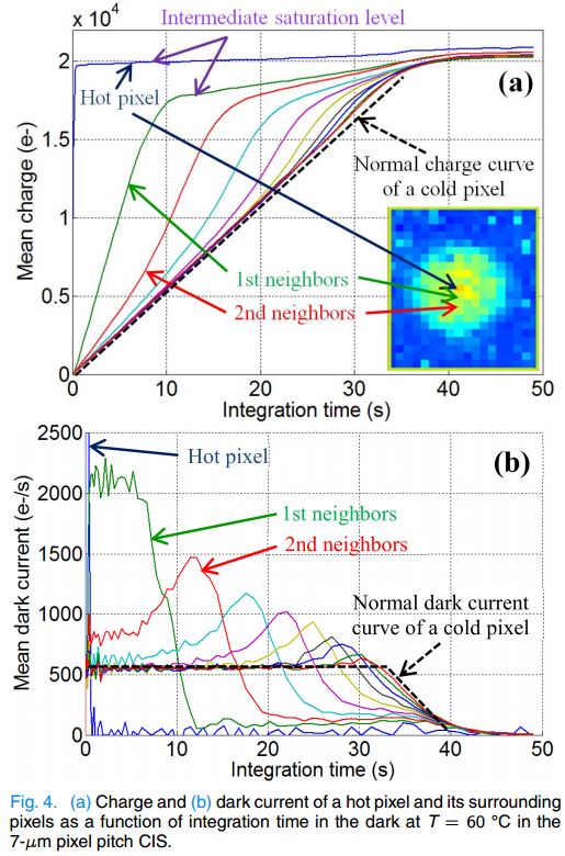
"This paper demonstrates the existence of dark current blooming in pinned photodiode (PPD) CMOS image sensors (CISs) with the support of both experimental measurements and TCAD simulations. It is usually assumed that blooming can appear only under illumination, when the charge collected by a pixel exceeds the full well capacity (FWC) (i.e., when the photodiode becomes forward biased). In this paper, it is shown that blooming can also appear in the dark by dark current leakage from hot pixels in reverse bias (i.e., below the FWC). The dark current blooming is observed to propagate up to nine pixels away in the experimental images and can impact hundreds of pixels around each hot pixel. Hence, it can be a major image quality issue for the state-of-the-art PPD CISs used in dark current limited applications, such as low-light optical imaging and should be considered in the dark current subtraction process. This paper also demonstrates that one of the key parameter for dark current optimization, the transfer gate bias during integration, has to be carefully chosen depending on the application because the optimum bias for dark current reduction leads to the largest dark current blooming effects."
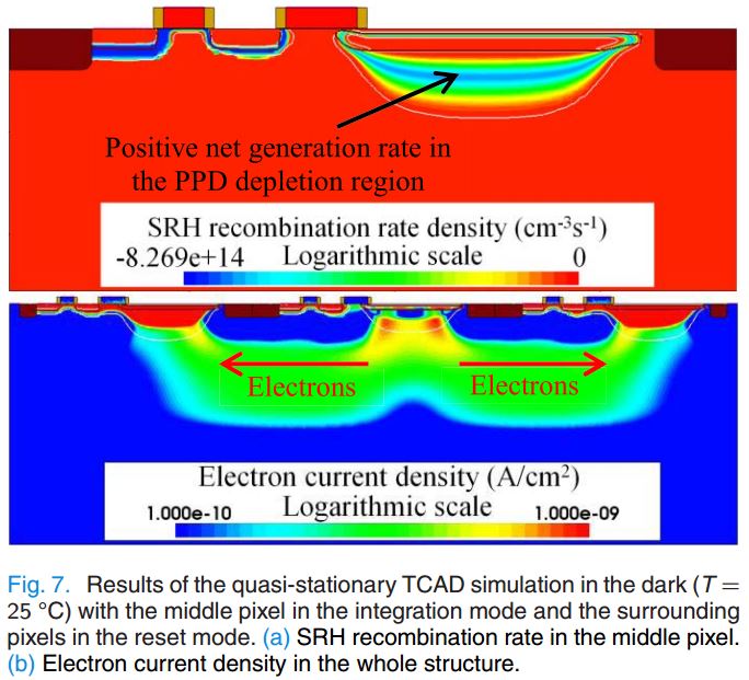
"The effect of the TG bias (VTG) during integration on the dark current blooming has been investigated (Fig. 9). A slight negative bias (−0.2 V in this paper) is usually chosen for low-light imaging because it ensures a very low mean dark current of the CIS. Indeed, the oxide interface under the TG is mainly accumulated with holes in that case, which neutralize the interface generation centers [15]. However, the potential barrier under the TG is higher than the potential barrier between the PPD and the epitaxy, because the substrate is grounded (0 V). Therefore, the dark current of the PPD is rather emitted toward the epitaxy than under the TG by thermionic emission, which leads to the dark current blooming (Fig. 9). If the TG is biased positively (+0.2 V in Fig. 9), which is a common light induced blooming countermeasure, the potential barrier under the TG becomes lower than toward the epitaxy and the dark current will rather diffuse under the TG (and will be collected by the floating diffusion) than toward the epitaxy. In that case, it can be seen in Fig. 9 that the dark current blooming is supressed. However, the mean dark current of the CIS is higher due to the depleted oxide interface under the TG."

I'm getting flashbacks from seeing this issue in at a past (sensor) company.
ReplyDeleteThis summary pretty much backs up our own findings.
It seems to me that the most important part is to find a good compromise between hotpixel blooming reduction and mean DC reduction for low light imaging!? Did anyone try this?
ReplyDelete- dkf
Can anyone pls tell me how to measure dark current of pixel using TCAD. What is the correct procedure to calculate it in TCAD.
ReplyDelete